* Two LVCMOS / LVTTL outputs
* Differential CLK, nCLK input pair
* CLK, nCLK pair can accept the following differential input levels: LVPECL, LVDS, LVHSTL, HC.
with limited board space. www.DataSheet4U.com
IC S
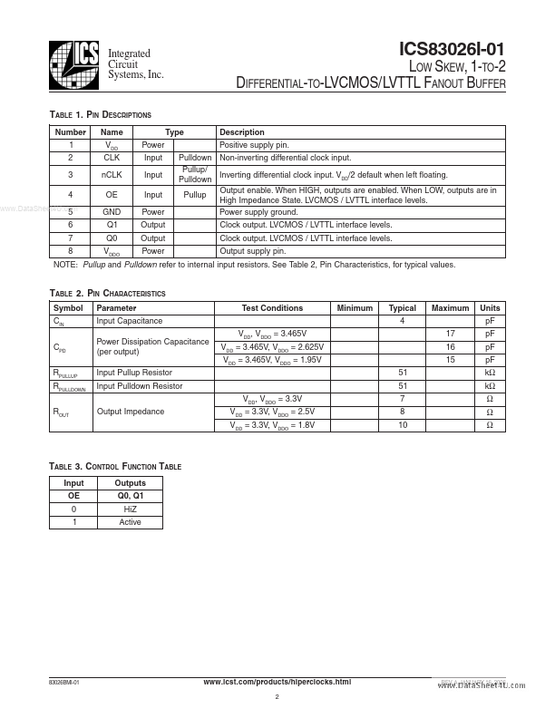
BLOCK DIAGRAM
PIN ASSIGNMENT
VDD CLK nCLK OE 1 2 3 4 8 7 6 5 VDDO .
The ICS83026I-01 is a low skew, 1-to-2 Differential-to-LVCMOS/LVTTL Fanout Buffer and HiPerClockS™ a member of the HiPerClockS ™ family of High Perfor mance Clock Solutions from ICS. The differential input can accept most differential signal types (L.
Image gallery
TAGS
Manufacturer
Related datasheet

